How MF do SMT for LED lights?
What is SMT?
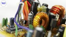
SMT production line, surface mount technology (SMT) is a new generation of electronic assembly technology developed from hybrid integrated circuit technology. It is characterized by using component surface mount technology and reflow soldering technology, and has become a new generation of assembly technology in electronic product manufacturing.
The wide application of SMT promotes the miniaturization and multifunction of electronic products, and provides conditions for mass production and low defect rate production. SMT is surface assembly technology, which is a new generation of electronic assembly technology developed from hybrid integrated circuit technology.
 Audited supplier
What is MF SMT process equipment ?
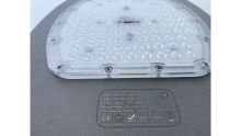
1. Formwork: (steel mesh)
Firstly, determine whether to process the template according to the designed PCB. If the patch elements on the PCB are only resistors and capacitors and are encapsulated above 1206, the solder paste can be coated with a needle cylinder or automatic dispensing equipment without making a template; When the PCB contains chips packaged with sot, SOP, PQFP, PLCC and BGA, and the packaging of resistance and capacitance is below 0805, a template must be made. The general template is divided into chemically etched copper template (low price, suitable for small batch and test, and the chip pin spacing is 0.635mm); Laser etched stainless steel template (high precision, high price, suitable for mass and automatic production lines, and the chip pin spacing is 0.5mm). For R & D, small batch production or spacing of 0.5mm, it is recommended to use etched stainless steel template; For mass production or laser cut stainless steel formwork with a spacing of 0.5mm. The overall dimension is 370 * 470 (unit: mm), and the effective area is 300 * 400 (unit: mm).

2. Silk screen printing: (high precision semi-automatic solder paste printing machine)
Its function is to use a scraper to leak solder paste or patch adhesive onto the PCB pad to prepare for the installation of components. The equipment used are manual silk printing table (screen printer), template and scraper (metal or rubber), which are located at the front of SMT production line. It is recommended to use medium-sized silk screen printing table and precision semi-automatic silk screen printing machine to fix the template on the silk screen printing table. Determine the position of PCB on the silk screen printing platform through the up, down, left and right knobs on the manual silk screen printing table and fix this position; Then place the PCB to be coated between the screen printing platform and the template, place the solder paste on the screen plate (at room temperature), keep the template parallel to the PCB, and evenly apply the solder paste on the PCB with a scraper. In the process of use, pay attention to the timely cleaning of the formwork with alcohol to prevent the solder paste from blocking the leakage of the formwork.

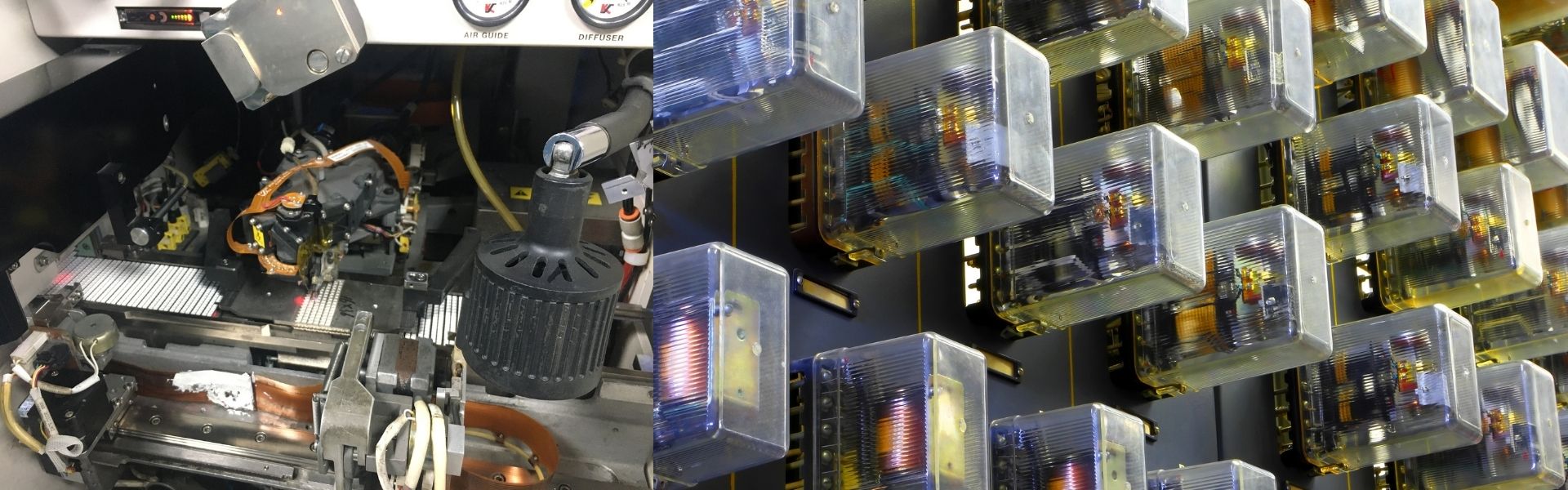
3. Mounting: (Korean high precision automatic multi-function Mounter)
Its function is to accurately install surface mount components to the fixed position of PCB. The equipment used is a mounter (automatic, semi-automatic or manual), a vacuum suction pen or tweezers, which is located behind the silk printing table in the SMT production line. For laboratory or small batch, it is generally recommended to use double pen head anti-static vacuum suction pen. In order to solve the problem of mounting and alignment of high-precision chips (chip pin spacing 0.5mm), it is recommended to use Samsung automatic multi-functional high-precision Mounter (model sm421 can improve efficiency and mounting accuracy). The vacuum suction pen can directly pick up the resistance, capacitance and chip from the component material rack. Because the solder paste has a certain viscosity, the resistance and capacitance can be directly placed at the required position; For the chip, a suction cup can be added on the vacuum pen head, and the suction force can be adjusted by the knob. Remember that no matter what components are placed, pay attention to the alignment position. If the position is misplaced, the PCB must be cleaned with alcohol, screen printed again, and the components must be placed again.
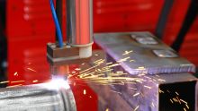
4. Reflow soldering:
Its function is to melt the solder paste and braze the surface mounted components and PCB firmly to achieve the electrical performance required by the design. It is precisely controlled in full accordance with the international standard curve, which can effectively prevent the thermal damage and deformation of PCB and components. The equipment used is a reflow soldering furnace (full-automatic infrared hot air reflow soldering furnace), which is located behind the mounter in the SMT production line.

5. Cleaning:
Its function is to remove the substances or welding residues that affect the electrical properties on the pasted PCB, such as flux. If cleaning free solder is used, it can generally not be cleaned. Products requiring low power consumption or good high frequency characteristics shall be cleaned, and general products can be free of cleaning. The equipment used is ultrasonic cleaning machine or manual cleaning with alcohol, and the position can not be fixed.

6. Inspection:
Its function is to inspect the welding quality and assembly quality of the pasted PCB. The equipment used includes magnifying glass and microscope, and the position can be configured in the appropriate place of the production line according to the needs of inspection.

7. Repair:
Its function is to rework the PCB with faults detected, such as tin ball, tin bridge, open circuit and other defects. The tools used are intelligent soldering iron, repair workstation, etc. Configure anywhere in the production line.

Audited supplier